TrendForce News operates independently from our research team, curating key semiconductor and tech updates to support timely, informed decisions.
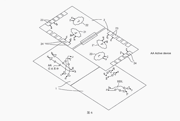
Backed by founder Ren Zhengfei’s belief that advanced packaging and stacking can keep China in the advanced chip race, Huawei has reportedly filed a patent for a quad-chiplet design—likely linked to its next-gen AI chip, the Ascend 910D, per Tom’s Hardware.
The report suggests that it could spell trouble for NVIDIA, as the layout echoes its quad-die Rubin Ultra. In addition, the move implies Huawei’s push into advanced packaging, which might aim to rival TSMC’s and help it bypass U.S. sanctions, the report adds.
In late April, the Wall Street Journal revealed that Huawei reached out to several Chinese tech firms to test the Ascend 910D’s feasibility, with the first samples expected by late May. Now, new patent details are shedding more light on the chip.
Bridge-style Links Mirror TSMC and Intel Designs
Notably, Tom’s Hardware names the patent’s chiplet interconnect design as one of the key highlight, adding that instead of a traditional interposer, Huawei’s patent hints at bridge-style links—similar to TSMC’s CoWoS-L or Intel’s EMIB with Foveros 3D. For AI training, the processor would also likely be paired with HBM-class memory, according to Tom’s Hardware.
This could be a turning point for China’s tech giants. While Huawei and SMIC lag in lithography and lack access to ASML’s advanced EUV machines, they may be catching up in advanced packaging—linking older-node chiplets to build high-performance systems, as noted by Tom’s Hardware.
Massive Size Could Be a Concern
However, if this patent is indeed the rumored Ascend 910D, Tom’s Hardware points out the chip could be massive. The single-chiplet 910B measures about 665 mm², so a quad-chiplet 910D could reportedly hit 2,660 mm². Moreover, the report notes since each 910B includes four HBM chiplets, with 16 HBM stacks (about 85 mm² each), the total DRAM area could swell to roughly 1,360 mm².
According to Tom’s Hardware, that puts the combined silicon footprint near 4,020 mm²—about five EUV reticle sizes by TSMC standards, a scale TSMC aims to support in volume by 2026.
Beyond that, can Huawei’s Ascend 910D truly outpace NVIDIA’s H100 in per-GPU performance? The world is watching closely.
Read more
(Photo credit: Huawei)